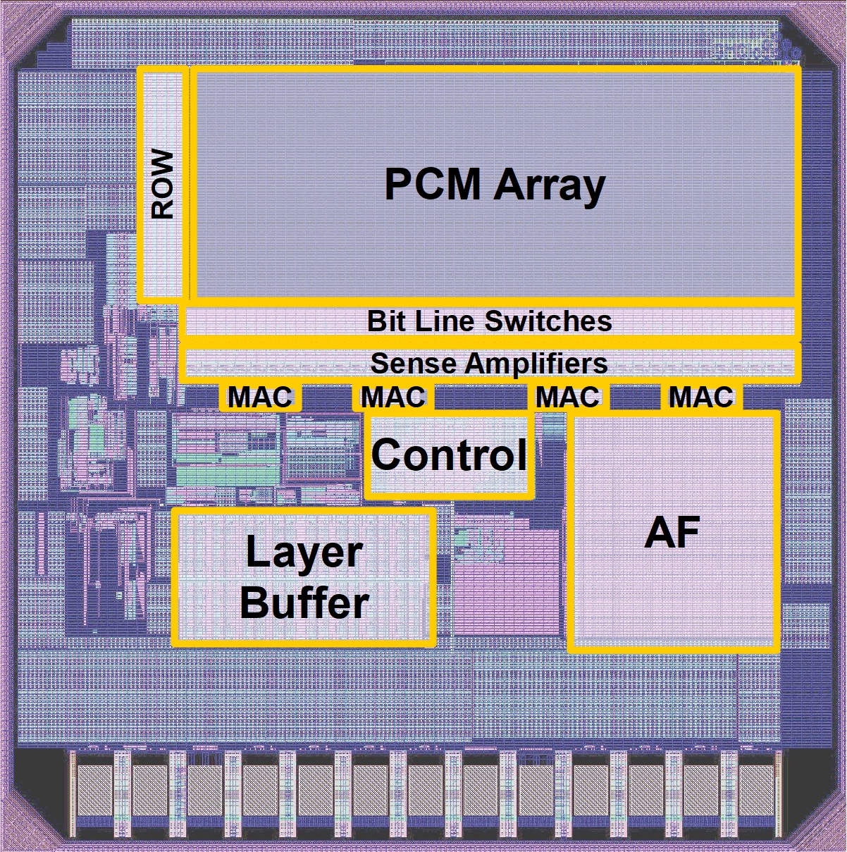
High-Performance Computing
Green Mountain Semiconductor brings a sophisticated expertise in memory and high speed I/Os design.
This allows us to maximize in-memory computation with the aim to reduce power and increase performance while leveraging the high parallelism inherent in the memory architectures.
Our company consists of a proficient team of experts in the field with the know-how to develop a full-fledged PHY on advanced technology nodes for the specific purpose of enabling high-speed data exchanges between memories and the CPU.