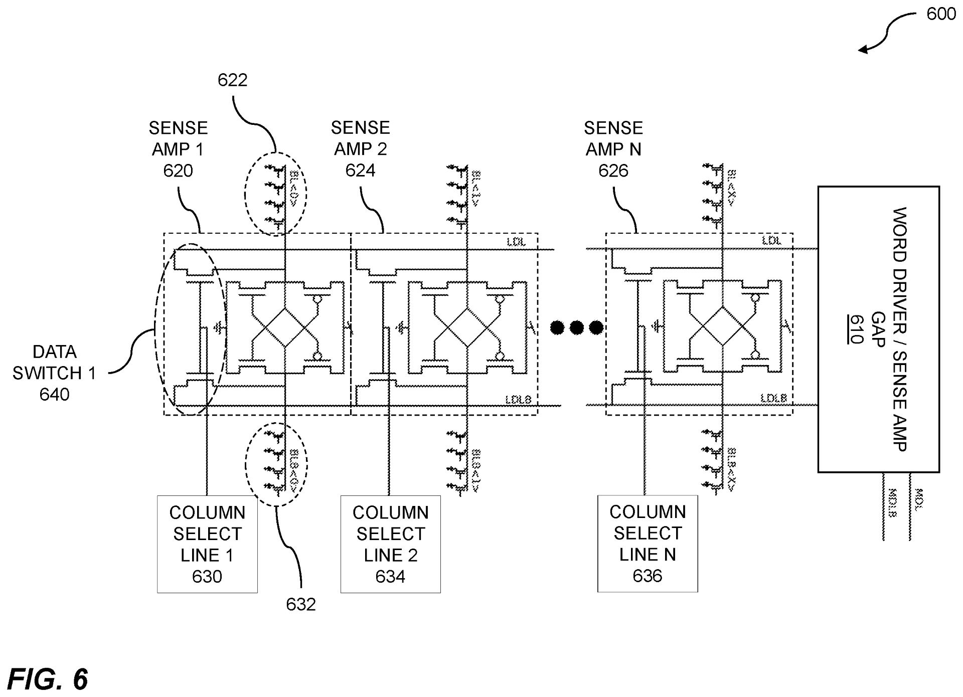
AI Circuit Design

GMS is able to develop custom compute-in-memory architectures from the ground up, based on deep roots in Memory Design (DRAM, SRAM, Emerging NVM). combined with fundamental research on ultra-low power in-memory neural networks for autonomous AI inferencing since 2016. After carefully selecting the related memory technologies and the corresponding foundry, GMS brings compelling value throughout the whole process, from the design scope assessment phase to the architecture, circuit design, simulation, layout, integration and application specific optimization stages.

In-Memory Computing

Green Mountain Semiconductor has a long history in memory design, both from within the company itself and through the prior work experience of our skilled team. Since 2015 we have worked on in-memory computation with the aim to reduce power and increase performance. Our expertise with commodity memory product development led us to realize the potential to leverage the high parallelism inherent in the memory architectures.

We have worked on two consecutive NSF grants to develop IP around in-memory search and artificial intelligence algorithms embedded into the memory hardware.

Image label and attribution

Previous Experience

  • Commodity DRAM design (LPDDR, DDR up to 2GB, 6.4GB/s)
  • SRAM macro design up to 128MBit
  • Emerging memories (STT MRAM, Phase Change Memory)
  • Memory PHY design in various technology nodes down to 7nm
  • Development of product prototypes (256M LPDDR2-NV and 32M SPI Flash-replacement) with error correction code (ECC)
  • Specialty memory R&D (ultra low temperature DRAM circuits)

Patented Technology

Green Mountain Semiconductor has several patents granted and pending in the field of commodity memory architecture, error correction code and in-memory high-parallel data processing.

White Papers

Our firm has authored a multitude of comprehensive white papers. We invite you to explore our library. For full access and the ability to download any of our papers, please submit a request for access.

Co-design of a novel CMOS highly parallel, low-power, multi-chip neural network accelerator

Why do security cameras, sensors, and Siri use cloud servers instead of on-board computation? The lack of very low power, high-performance chips greatly limits the ability to field untethered edge devices. We present the NV-1, a new low-power ASIC AI processor that greatly accelerates parallel processing (10X) with dramatic reduction in energy consumption (>100X), via many parallel combined processor-memory units, i.e., a drastically non-von-Neumann architecture, allowing very large numbers of independent processing streams without bottlenecks due to typical monolithic memory. The current initial prototype fab arises from a successful co-development effort between algorithm- and software-driven architectural design and VLSI design realities. An innovative communication protocol minimizes power usage, and data transport costs among nodes were vastly reduced by eliminating the address bus, through local target address matching. Throughout the development process, the software/architecture team was able to innovate alongside the circuit design team’s implementation effort. A digital twin of the proposed hardware was developed early on to ensure that the technical implementation met the architectural specifications and, indeed, the predicted performance metrics have now been thoroughly verified in real hardware test data. The resulting device is currently being used in a fielded edge sensor application. Additional proofs of principle are in progress, demonstrating the proof on the ground of this new real-world extremely low-power high-performance ASIC device.

May 15, 2024

Opportunities and Limitations of in-Memory Multiply-and-Accumulate Arrays

In-memory computing is a promising solution to solve the memory bottleneck problem which becomes increasingly unfavorable in modern machine learning systems. In this paper, we introduce an architecture of random access memory (RAM) incorporating deep learning inference abilities. Due to the digital nature of this design, the architecture can be applied to a variety of commercially available volatile and non-volatile memory technologies. We also introduce a multi-chip architecture to accommodate for varying network sizes and to maximize parallel computing ability. Moreover, we discuss the opportunities and limitations of in-memory computing as future neural networks scale, in terms of power, latency and performance. To do so, we applied this architecture to various prevalent neural networks, e.g. Artificial Neural Network (ANN), Convolutional Neural Network (CNN) and Transformer Network and compared the results.

January 01, 2021

Design and Testing Considerations of an In-Memory AI Chip

In-memory computing is a propitious solution for overcoming the memory bottleneck for future computer systems. In this work, we present the testing and validation considerations for a programmable artificial neural network (ANN) integrated within a phase change memory (PCM) chip, featuring a Nor- Flash compatible serial peripheral interface (SPI). In this paper, we introduce our method for validating the circuit components specific to the ANN application. In addition, high-density in- memory multi-layer ANNs cannot be manufactured without testing and repair of the memory array itself. Therefore, design for testability (DFT) features commonly used in commodity or embedded memory products must be maintained as well. The combination of these two test/characterization steps alleviates the need to test the actual inference functionality in hardware.

January 01, 2020